S17: Smart Health Gear
Contents
Grading Criteria
- How well is Software & Hardware Design described?
- How well can this report be used to reproduce this project?
- Code Quality
- Overall Report Quality:
- Software Block Diagrams
- Hardware Block Diagrams
- Schematic Quality
- Quality of technical challenges and solutions adopted.
Project Title
Smart Health Gear
Abstract
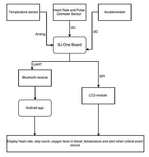
Smart Health Gear is a wearable device which will help in monitoring various aspects of a person's health like heart rate, foot steps count and body temperature. It will come with a compatible android application which will notify the user on completion of daily activities and log all the data from the Smart Health Gear to provide a history chart.
Objectives & Introduction
Show list of your objectives. This section includes the high level details of your project. You can write about the various sensors or peripherals you used to get your project completed.
Team Members & Responsibilities
- Aniket Dali
- Jean Mary
- Manoj Ramesh Rao
- Neha Biradar
- Sushma Macha
Schedule
Show a simple table or figures that show your scheduled as planned before you started working on the project. Then in another table column, write down the actual schedule so that readers can see the planned vs. actual goals. The point of the schedule is for readers to assess how to pace themselves if they are doing a similar project.
| Week# | Date | Task | Comments |
|---|---|---|---|
| 1 | 3/2 | Submission of Project Proposals | Completed |
| 2 | 3/15 | Gathering requirements | Completed |
| 3 | 3/30 | Finalizing and documenting project requirements | Completed |
| 4 | 4/5 | Initiate research on components and start research/development on algorithms to read sensor values. | In progress |
| 5 | 4/8 | Initiate development of sensor and IO modules in software. | In progress |
| 6 | 4/16 | Finish component procurement and start PCB design. Start research on strategies for unit and integration testing. | In progress |
| 7 | 4/18 | Designing code architecture and interfaces. Prepare test plan to unit test sensor and IO modules. | |
| 8 | 4/23 | Finish unit test plan. Finish PCB design and Place and order for PCB fabrication . | |
| 9 | 4/24 | Finish and document code architecture and initialize interfaces provided to RTOS application. Initiate designing of Android application. | |
| 10 | 4/25 | Development of RTOS application to control sensor and IO modules. | |
| 11 | 4/27 | Unit testing of sensor and IO modules and updating results. Initiate preparation of integration test plan. | |
| 12 | 4/30 | Bug fixing and re-testing. Initiate Unit testing of RTOS application. | |
| 13 | 5/2 | Bug fixing and re-testing for unit test phase. | |
| 14 | 5/4 | Integration testing of sensor modules and RTOS application and update results. | |
| 15 | 5/8 | Bug fixing and re-testing. Initiate PCB testing. | |
| 16 | 5/12 | Bugs fixing and re-testing for integration and PCB. | |
| 17 | 5/14 | Start System testing. | |
| 18 | 5/16 | Bug fixing and re-testing.Initiate documentation of project report. | |
| 19 | 5/19 | Bug fixing and re-testing.Finish project documentation. | |
| 20 | 5/20 | Prepare release note. Ready for demo. | |
| 21 | 5/21-5/22 | Buffer. | |
| 22 | 5/23 | Demo. |
Parts List & Cost
| Item# | Part | Manufacturer | Part number | Cost($) |
|---|---|---|---|---|
| 1 | SJ One Board | Preet | n/a | 80.00 |
| 2 | Heart-Rate Monitor and Pulse Oximeter Sensor | Maxim | MAXREFDES117 | 20.00 |
| 3 | HC-06 wireless bluetooth transceiver | Banggood | Datasheet | 6.55 |
| 4 | 10K Precision Epoxy Thermistor - 3950 NTC | Adafruit | Lookup Table | 4.00 |
| 5 | LCD module | Aliexpress | SEN-10988 | 32.30 |
| 6 | Hardware | Excess Solution | Berg strips, Jumper wires, Connectors, Standoffs | 5.00 |
| 7 | 9V Battery | Amazon | 32.30 |
- Total Cost: 153.79$
Design & Implementation
The design section can go over your hardware and software design. Organize this section using sub-sections that go over your design and implementation.
Printed Circuit Board
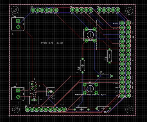
The PCB design was one of the challenging part of this project. The PCB design was created in Autodesk Eagle v8.1.0. Before proceeding with the schematic, we had decided to design a PCB that matches with the size of the SJ one board such that it could be mounted over it. Considering designing a wearable device, we had to keep in mind the form factor of the PCB. Initially we designed a PCB which turned out to be four-layer PCB including the blood pressure monitoring subsystem. However due to budget constraints we had to give up the blood pressure system as printing the same required a licensed version of Eagle.
Before starting the PCB schematic design, we decided on the location of sensors as it was vital for a wearable health monitoring device with a LCD display facing the user. Since surface mount soldering was not an option we decided to design the schematic with through hole connections. Another challenging part for our design was the libraries needed for schematic design. Since we didn’t have libraries for heart rate sensors, we had to design by creating it from scratch. However, we had some libraries from sparkfun, Eagle and Adafruit, the entire process took most of our time.
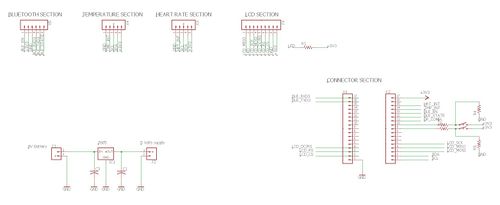
The first step in PCB design is to import all the libraries of the components that we would be using and create a schematic using the same. We made use of the Dimension tool in Eagle to match the PCB size with that of the SJ one board. We created the schematic by placing the required components and wiring them. The tutorial on Sparkfun website was very helpful in designing the same. It was very important for to ensure that all connections are verified properly before it gets printed. This was done using “DRC” Design Rule Check in Eagle which would show if any consistent errors existed.
EAGLE Schematic
EAGLE Connector List
| Section | Connector | Library | Package | Device |
|---|---|---|---|---|
| Power Connector | 2x2-pin | SparkFun-Connectors | SCREWTERMINAL-3.5MM-2 | CONN_023.5MM (CONN_02) |
| SJ-One Board | 2x17-pin | SparkFun-Connectors | 1X17 | CONN_17 |
| Bluetooth Module | 1x6-pin | SparkFun-Connectors | 1X06 | CONN_06SILK_FEMALE_PTH (CONN_06) |
| Temperature Sensor | 1x5-pin | SparkFun-Connectors | 1X05 | CONN_05 |
| Heart Rate Sensor | 1x5-pin | SparkFun-Connectors | 1X05 | CONN_05 |
| LCD Section | 1x9-pin | SparkFun-Connectors | 1X09 | CONN_09 |
| Resistor | 5x2-pin | resistor | 0207/7 | R-US_0207/7 (R-US_) |
| Capacitor | 2x2-pin | rcl | C025-050X050 | C-US025-050X050 (C-US) |
| Switch | 2x4-pin | SparkFun-Switches | TACTILE_SWITCH_PTH_6.0MM | MOMENTARY-SWITCH-SPST-PTH-6.0MM (MOMENTARY-SWITCH-SPST) |
| LM7805 Regulator IC | 1x3-pin | v-reg | 78LXX | 78LXX |
Once the schematic is created that can be easily converted to Board Layout using the Generate/Switch to board option in Eagle. But this would create the board by randomly placing the parts at different locations. Since we had to have an LCD mount over the PCB as well as match the 17x2 connectors with that of SJ one board we created the design accordingly. After ensuring that everything was in place we placed order for the PCB and verified the same again using a multi-meter if all the connections were correct.
Hardware Design
Discuss your hardware design here. Show detailed schematics, and the interface here.
Heart Rate Sensor
Temperature Sensor
LCD
The LCD interface is used to display the information collected from all the sensors to the user. ILI9340 supports a TFT liquid crystal display with a resolution of 240RGB*320 dots. It supports full color, 8-color display mode and sleep mode as well as precise power control by software. Moving pictures can be independently displayed in an address window such that only that window displays moving picture even if the rest of space displays static data.
SPI0 peripheral is initialized as master and the LCD is interfaced as slave. LCD is initialized by sending commands to set the power, frame rate, pixel depth etc., The display is activated by giving vcc to its LED input. The commands are sent along with parameters via SPI in the pre-defined sequence in order to perform actions like setting the row and column index to position the pixel appropriately. The data and commands are distinguished by d/cx input pin which can be written 1 for data and 0 for command.
To display characters or lines or any shapes we need to fill up the screen pixel by pixel by positioning the pixels in appropriate location using the row set and column set commands. The commands and its parameters are sent to LCD via SPI interface and are then followed by the data i.e., the pixel color. There are two screens – The default screen will display the Time Stamp and the next screen will display the sensor data. These two screens are swapped either after timeout or after a button press. A timer is initialized to count every micro second and after counting 300 times the timer gives a binary semaphore which is captured a task which swaps the screens. The LCD is interfaced to two switches using two GPIO pins. One switch is used to power off and power on the LCD and the other one is used to navigate between the two screens.
There are two tasks running, Display Task, Button Task at equal priority. The Display Task is waiting for a screen_change semaphore which is given by timer or button press. It checks for any update to be made in the clock screen i.e., if any of sec, min, hour, day, month or year is changed if so it updates the same. If and when the semaphore is given the task takes it and changes the screen based on the value of a variable which represents the current screen. Button Task is waiting on a sensor_button semaphore which is released by an interrupt triggered by the button press.
Bluetooth Module
Software Design
Show your software design. For example, if you are designing an MP3 Player, show the tasks that you are using, and what they are doing at a high level. Do not show the details of the code. For example, do not show exact code, but you may show psuedocode and fragments of code. Keep in mind that you are showing DESIGN of your software, not the inner workings of it.
Implementation
This section includes implementation, but again, not the details, just the high level. For example, you can list the steps it takes to communicate over a sensor, or the steps needed to write a page of memory onto SPI Flash. You can include sub-sections for each of your component implementation.
Testing & Technical Challenges
Describe the challenges of your project. What advise would you give yourself or someone else if your project can be started from scratch again? Make a smooth transition to testing section and described what it took to test your project.
Include sub-sections that list out a problem and solution, such as:
My Issue #1
Discuss the issue and resolution.
Conclusion
Conclude your project here. You can recap your testing and problems. You should address the "so what" part here to indicate what you ultimately learnt from this project. How has this project increased your knowledge?
Project Video
Upload a video of your project and post the link here.
Project Source Code
References
Acknowledgement
Any acknowledgement that you may wish to provide can be included here.
References Used
List any references used in project.
Appendix
You can list the references you used.


