Difference between revisions of "F16: Piano Glove"
(→Hardware & Software Tradeoffs) |
(→Visualization Development) |
||
| (223 intermediate revisions by the same user not shown) | |||
| Line 1: | Line 1: | ||
| − | |||
| − | |||
| − | |||
| − | |||
| − | |||
| − | |||
| − | |||
| − | |||
| − | |||
| − | |||
| − | |||
| − | |||
== Project Title == | == Project Title == | ||
| − | <center><h3> OVS: Piano | + | <center><h3> OVS: Piano Gloves </h3></center> |
== Abstract == | == Abstract == | ||
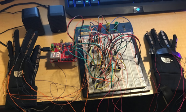
| − | Music is in our everyday lives. Unfortunately, it is expensive to learn how to play an instrument. Therefore, we have decided to create '''Piano Gloves''' which can stand as a cheaper alternative to purchasing a Piano. This is a device that generates a | + | Music is in our everyday lives. Unfortunately, it is expensive to learn how to play an instrument. Therefore, we have decided to create '''Piano Gloves''' which can stand as a cheaper alternative to purchasing a Piano. This is a device that generates a fun piano-key note based on which finger is flexed. Our project gives the user flexibility in the types of notes that they would like to play. For instance, the user may select a ''Classic'' or ''8-bit'' mode to access different note types. Please view our video at the bottom of the page for a live demonstration. |
| + | |||
| + | |||
| + | [[File:CmpE146 F16 T2 PianoGloves.PNG | 600px |center | <center> '''Figure 1. Completed Project '''</center>]] | ||
== Objectives & Introduction == | == Objectives & Introduction == | ||
| Line 25: | Line 16: | ||
* Sew Flex Sensors onto Gloves | * Sew Flex Sensors onto Gloves | ||
* Create our own ADC circuit using OP-AMPS to handle 10 Analog inputs (1 per each finger) | * Create our own ADC circuit using OP-AMPS to handle 10 Analog inputs (1 per each finger) | ||
| − | * | + | * Configure the onboard DAC of the SJOne Board, as well as initializing GPIO ports |
| + | * Perform a full system integration for a finalized prototype | ||
| + | |||
| + | '''Optional Tasks''' | ||
* Create a Real Time visualization based on which finger is flexed | * Create a Real Time visualization based on which finger is flexed | ||
| − | |||
=== Team Members & Responsibilities === | === Team Members & Responsibilities === | ||
| Line 36: | Line 29: | ||
* Algorithm Development | * Algorithm Development | ||
* System Integration, Verification, and Validation Testing | * System Integration, Verification, and Validation Testing | ||
| + | * Visualization Development | ||
[https://www.linkedin.com/in/benjamin-vuong-87892087 Benjamin Vuong] | [https://www.linkedin.com/in/benjamin-vuong-87892087 Benjamin Vuong] | ||
* Algorithm Development | * Algorithm Development | ||
| + | * Software Development | ||
| + | * Research on Music Frequencies and Design of Simulated Soundwaves | ||
* Device Driver Implementation | * Device Driver Implementation | ||
* System Integration, Verification, and Validation Testing | * System Integration, Verification, and Validation Testing | ||
== Schedule Overview == | == Schedule Overview == | ||
| − | |||
<center> | <center> | ||
| Line 87: | Line 82: | ||
| 11/18/16 | | 11/18/16 | ||
| Status Update: Demo First Round of Prototyping | | Status Update: Demo First Round of Prototyping | ||
| − | | | + | | Complete |
| − | | | + | | 11/18/16 |
|- | |- | ||
! scope="row"| 6 | ! scope="row"| 6 | ||
| Line 94: | Line 89: | ||
| 11/25/16 | | 11/25/16 | ||
| Interface Modules and Perform System Design Verification/Validation Testing | | Interface Modules and Perform System Design Verification/Validation Testing | ||
| − | | | + | | Complete |
| − | | | + | | 11/30/16 |
|- | |- | ||
! scope="row"| 7 | ! scope="row"| 7 | ||
| Line 101: | Line 96: | ||
| 12/02/16 | | 12/02/16 | ||
| Continue Validation and Optimize System | | Continue Validation and Optimize System | ||
| − | | | + | | Complete |
| − | | | + | | 12/05/16 |
|- | |- | ||
! scope="row"| 8 | ! scope="row"| 8 | ||
| Line 108: | Line 103: | ||
| 12/20/16 | | 12/20/16 | ||
| Finalize Design and Prepare for Demo | | Finalize Design and Prepare for Demo | ||
| − | | | + | | Complete |
| − | | | + | | 12/18/16 |
| − | |||
| − | |||
|} | |} | ||
| Line 117: | Line 110: | ||
== Parts List & Cost == | == Parts List & Cost == | ||
| − | |||
<center> | <center> | ||
| Line 129: | Line 121: | ||
|- | |- | ||
! scope="row"| 1 | ! scope="row"| 1 | ||
| − | | | + | | SJOne Board |
| [https://www.linkedin.com/in/preetpalkang Preet] | | [https://www.linkedin.com/in/preetpalkang Preet] | ||
| 1 | | 1 | ||
| Line 137: | Line 129: | ||
| Flex Sensors | | Flex Sensors | ||
| [http://www.mouser.com/ProductDetail/Spectra-Symbol/FS-L-0055-253-ST/?qs=avFSO%252b7Rp3iBf0lmBypxdg%3D%3D Mouser] | | [http://www.mouser.com/ProductDetail/Spectra-Symbol/FS-L-0055-253-ST/?qs=avFSO%252b7Rp3iBf0lmBypxdg%3D%3D Mouser] | ||
| − | | | + | | 25 |
| $6.45 | | $6.45 | ||
|- | |- | ||
! scope="row"| 3 | ! scope="row"| 3 | ||
| − | |||
| − | |||
| − | |||
| − | |||
| − | |||
| − | |||
| MCP6242-E/P OPAMP | | MCP6242-E/P OPAMP | ||
| [http://www.mouser.com/search/ProductDetail.aspx?r=579-MCP6242-E%2fP Mouser] | | [http://www.mouser.com/search/ProductDetail.aspx?r=579-MCP6242-E%2fP Mouser] | ||
| Line 152: | Line 138: | ||
| $0.36 | | $0.36 | ||
|- | |- | ||
| − | ! scope="row"| | + | ! scope="row"| 4 |
| 3.5mm Audio Jack | | 3.5mm Audio Jack | ||
| − | | [https://www. | + | | [https://www.sparkfun.com/products/8032 SparkFun] |
| 1 | | 1 | ||
| $0.95 | | $0.95 | ||
|- | |- | ||
| − | ! scope="row"| | + | ! scope="row"| 5 |
| Gloves | | Gloves | ||
| Northface | | Northface | ||
| Line 164: | Line 150: | ||
| N/A | | N/A | ||
|- | |- | ||
| − | ! scope="row"| | + | ! scope="row"| 6 |
| Misc Parts (Wires, Resistors, Capacitors etc) | | Misc Parts (Wires, Resistors, Capacitors etc) | ||
| Personal | | Personal | ||
| Line 171: | Line 157: | ||
|} | |} | ||
| + | </center> | ||
| + | |||
| + | * '''NOTE:''' Exact resistance values are not given for this project because they are different for each circuit. If you were to try to implement this project on your own, you would need to recalculate your individual resistances based on your respective Flex Sensors. | ||
| − | |||
=== Software Used === | === Software Used === | ||
| + | * For this project, we implemented FreeRTOS which was provided to us by our instructor Preet. A download and tutorial of how to use it can be found [http://www.socialledge.com/sjsu/index.php?title=Development_Package here]. | ||
== Hardware Design & Interface == | == Hardware Design & Interface == | ||
| − | + | ||
=== Hardware Schedule === | === Hardware Schedule === | ||
| − | |||
<center> | <center> | ||
| Line 204: | Line 192: | ||
| 11/4/16 | | 11/4/16 | ||
| 11/11/16 | | 11/11/16 | ||
| − | | Design and Interface Schmitt Trigger Circutry w/ | + | | Design and Interface Schmitt Trigger Circutry w/SJOne Board <br>Create PCB Schematic<br/> |
| Completed | | Completed | ||
| 11/11/16 | | 11/11/16 | ||
| Line 212: | Line 200: | ||
| 11/11/16 | | 11/11/16 | ||
| 11/18/16 | | 11/18/16 | ||
| − | | Sew Flex Sensors onto Gloves and Interface w/Development Board <br | + | | Sew Flex Sensors onto Gloves and Interface w/Development Board <br>Status Update: Demo First Round of Prototyping <br/> |
| Complete | | Complete | ||
| 11/18/16 | | 11/18/16 | ||
| Line 220: | Line 208: | ||
| 11/18/16 | | 11/18/16 | ||
| 11/25/16 | | 11/25/16 | ||
| − | | Integrate Hardware and Software, Perform System Design Verification/Validation Testing | + | | Integrate Hardware and Software, Perform System Design Verification/Validation Testing |
| Complete | | Complete | ||
| − | | | + | | 11/25/16 |
| | | | ||
|- | |- | ||
| Line 229: | Line 217: | ||
| 12/02/16 | | 12/02/16 | ||
| Continue Validation and Optimize System | | Continue Validation and Optimize System | ||
| − | | | + | | Complete |
| − | | | + | | 12/05/16 |
| | | | ||
|- | |- | ||
| Line 237: | Line 225: | ||
| 12/20/16 | | 12/20/16 | ||
| Finalize Design and Prepare for Demo | | Finalize Design and Prepare for Demo | ||
| − | | | + | | Complete |
| − | | | + | | 12/18/16 |
| | | | ||
| Line 251: | Line 239: | ||
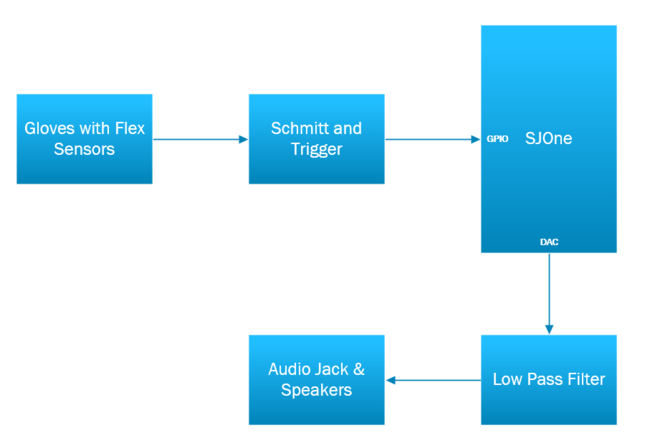
The following diagram is a high-level overview of our system. It is depicts the general structure of our design. In addition to that, it also demonstrates a generalization of the major system components that were used as well as their relationship among each other. | The following diagram is a high-level overview of our system. It is depicts the general structure of our design. In addition to that, it also demonstrates a generalization of the major system components that were used as well as their relationship among each other. | ||
| − | + | [[File:CmpE146 F16 T2 BlockDiagram.PNG | 650px | center| <center> '''Figure 1. Hardware Block Diagram: System Overview '''</center>]] | |
| − | [[File: | + | ==== Flex Sensors ==== |
| + | |||
| + | [[File:CmpE146 F16 T2 FlexSensor.PNG |thumb |left | <center> '''Figure 1. Flex Sensor '''</center>]] | ||
* ''' How they work''' | * ''' How they work''' | ||
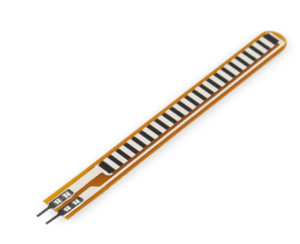
| + | A Flex Sensor is a ''passive'' device that can detect bending or moving. The resistance of the flex sensor changes whenever the metal pads (the side with the black stripe) are bent outward. As seen in Figure 1, the side with the thick black strips in the positive end and the side with the thin white strip is ground. | ||
* ''' How we used them''' | * ''' How we used them''' | ||
| − | For this project, 10 Flex Sensors were used. Each | + | For this project, 10 Flex Sensors were used. Each Flex Sensor was individually hand-sewn onto a finger of the gloves. These sensors were used to detect finger movement by triggering a certain voltage threshold when a finger was flexed to a certain degree ('''more of this will be explain in the section below'''). A voltage divider was used to discover the variably changing resistance in the Flex Sensor. In other words, by forming a voltage dividing circuit, we were able to determine the resistance in response to a finger movement (Rflex) that was proportional to the voltage output. (If you are unfamiliar with voltage dividers, please find a quick tutorial along with the mathematical equations [https://learn.sparkfun.com/tutorials/voltage-dividers here].) |
| + | |||
| + | * '''NOTE:''' Since each flex sensors resistance is slightly different, an individual voltage divider circuit was prepared for each sensor. | ||
| + | |||
| + | |||
| + | [[File:CmpE146 F16 T2 VoltageDivider.png |thumb |right | <center> '''Figure 2. Flex Sensor Schematic '''</center>]] | ||
| + | |||
| + | |||
| + | * '''Flex Sensor Hook Up''' | ||
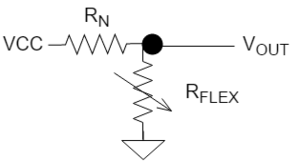
| + | As seen in '''Figure 2''', a voltage dividing circuit was used to interface with the Flex Sensor. First, we must ground our device, so the ground end of the sensor was attached to ground. Next a resistor (Rn) was connected to VCC and the other end of it was connected to the positive end of the sensor. Afterwards, we placed an output wire in between the positive end of the sensor and the resistor to get the output voltage of the device. This was considered Vout (or our analog output) that was fed into our Schmitt and Trigger Circuit as mentioned below. | ||
==== Schmitt and Trigger ==== | ==== Schmitt and Trigger ==== | ||
| − | |||
| − | *< | + | * ''' How it Works ''' |
| + | [[File:CmpE146 F16 T2 SchmittWave.PNG |thumb | right |upright=2 | <center>[https://www.youtube.com/watch?v=Nrp8OgQLAlw&feature=youtu.be '''Figure 3. Schmitt and Trigger Graphical Overview''']</center>]] | ||
| − | + | The Schmitt and Trigger circuit is a comparator with ''hysteresis''. Hysteresis is the "dependence of the state of a system based on its history". In other words, it helps filter out signals so that the output reacts less reapidly than it normally would by using its previous output. It's a type of "memory" for the circuit. For this circuit in particular, it aids in preventing unwanted and frequent switching by cancelling out the noise. A demonstration of this can be seen in '''Figure 3'''. This is accomplished this by applying a positive feedback into the non-inverting terminal of the differential amplifier. By doing this, we are able to see if the circuit has "triggered" or hit a certain threshold (our threshold was between 1.1v and 2.2v). Below in '''Figure 4''' is a schematic for the Schmitt and Trigger circuit that was used for this project. | |
| − | [[File: | + | [[File:General Schmitt Trigger.png |thumb |center |upright=2 | <center>'''Figure 4. General Schmitt Trigger Schematic'''</center>]] |
| + | [[File:SchmittTrigger.png |thumb |center |upright=3 | <center>'''Figure 5. Detailed on-chip Schmitt Trigger Schematic (This image shows two Schmitt Trigger Circuits implemented on 1 MCP6242-E/P OP AMP'''</center>]] | ||
| + | * ''' How we used it ''' | ||
| + | As seen in '''Figure 5''', the Schmitt and Trigger Circuit was implemented with a MCP6242-E/P OP AMP. It was used to convert the Analog Output of the Flex Sensors into a Digital Signal. This Analog to Digital Conversion (ADC) was done so that the SJOne MCU could interpret the input signal using a GPIO port and then determine what to do with it. Since there were 10 signals that needed an ADC, '''Figure 5''' was created a total of 5 times to account for producing 10 Digital Outputs (DO). | ||
| − | * ''' | + | *<font color=red>'''Design Choice'''</font>: We decided to create our own ADC circuit because of the limited availability on the SJOne board. There are simply not enough ADC pins to perform our task, as we would need 10 ADC pins. |
| − | |||
| − | ==== | + | ==== SJOne Board ==== |
| + | |||
| + | <center>A detailed description of the SJOne Board and it's capabilities can be found [http://www.socialledge.com/sjsu/index.php?title=SJ_One_Board '''here''']. </center> | ||
| + | |||
| + | |||
| + | [[File:CmpE146 F16 T2 SJONE.png | frame | center | <center> '''Figure 6. SJOne Board '''</center>]] | ||
| + | |||
| + | |||
| + | ===== General Purpose Input/Output (GPIO) ===== | ||
| + | |||
| + | As mentioned previously, GPIO pins from the SJOne Board were used to interpret the incoming signals produced from the Schmitt and Trigger. Below is a Pin Connectivity Table depicting the Pins we used, as well as their functionality. | ||
| + | |||
| + | <center> | ||
| + | '''GPIO: Pin Connectivity Table''' | ||
| − | |||
{| class="wikitable" | {| class="wikitable" | ||
|- | |- | ||
| − | ! scope="col"| | + | ! scope="col"| ITEM |
| − | ! scope="col"| | + | ! scope="col"| PORT.PIN |
| − | ! scope="col"| | + | ! scope="col"| DESCRIPTION |
| − | ! scope="col"| | + | ! scope="col"| DIRECTION |
| − | ! scope="col"| | + | ! scope="col"| CONNECTION |
|- | |- | ||
| + | ! scope="row"|1 | ||
| + | | P0.0 | ||
| + | | GPIO | ||
| + | | INPUT | ||
| + | | LEFT THUMB | ||
|- | |- | ||
| − | | | + | ! scope="row"| 2 |
| − | | | + | | P0.1 |
| − | | | + | | GPIO |
| + | | INPUT | ||
| + | | LEFT INDEX | ||
|- | |- | ||
| + | ! scope="row"| 3 | ||
| + | | P0.29 | ||
| + | | GPIO | ||
| + | | INPUT | ||
| + | | LEFT MIDDLE | ||
|- | |- | ||
| − | | | + | ! scope="row"| 4 |
| − | | | + | | P0.30 |
| − | | | + | | GPIO |
| + | | INPUT | ||
| + | | LEFT RING | ||
|- | |- | ||
| + | ! scope="row"| 5 | ||
| + | | P1.19 | ||
| + | | GPIO | ||
| + | | INPUT | ||
| + | | LEFT PINKY | ||
|- | |- | ||
| − | | | + | ! scope="row"| 6 |
| − | | | + | | P1.20 |
| − | | | + | | GPIO |
| + | | INPUT | ||
| + | | RIGHT THUMB | ||
|- | |- | ||
| + | ! scope="row"| 7 | ||
| + | | P1.22 | ||
| + | | GPIO | ||
| + | | INPUT | ||
| + | | RIGHT INDEX | ||
|- | |- | ||
| − | | | + | ! scope="row"| 8 |
| − | | | + | | P1.23 |
| − | | | + | | GPIO |
| + | | INPUT | ||
| + | | RIGHT MIDDLE | ||
| + | |- | ||
| + | ! scope="row"| 9 | ||
| + | | P1.28 | ||
| + | | GPIO | ||
| + | | INPUT | ||
| + | | RIGHT RING | ||
| + | |- | ||
| + | ! scope="row"| 10 | ||
| + | | P1.29 | ||
| + | | GPIO | ||
| + | | INPUT | ||
| + | | RIGHT PINKY | ||
|} | |} | ||
| − | + | </center> | |
| − | |||
| − | |||
| − | |||
===== Digital to Analog Converter (DAC) ===== | ===== Digital to Analog Converter (DAC) ===== | ||
| − | + | Below is a DAC connectivity table demonstrating the Pin Out of the DAC on the SJOne Board. Additionally, a block diagram has been provided to show how the DAC was interfaced with the Low Pass Circuit. | |
| − | + | <center> | |
| + | '''DAC: Pin Connectivity Table''' | ||
| − | |||
| − | |||
| − | |||
| − | |||
{| class="wikitable" | {| class="wikitable" | ||
|- | |- | ||
| − | ! scope="col"| | + | ! scope="col"| ITEM |
| − | ! scope="col"| | + | ! scope="col"| PORT.PIN |
| − | ! scope="col"| | + | ! scope="col"| DESCRIPTION |
| − | | | + | ! scope="col"| CONNECTION |
| − | |||
| − | |||
| − | |||
| − | |||
| − | |||
| − | |||
| − | |||
| − | |||
| − | |||
| − | |||
| − | |||
| − | |||
| − | |||
| − | |||
|- | |- | ||
| − | | | + | ! scope="row"|1 |
| − | | | + | | P0.26 |
| − | | | + | | DAC |
| − | | | + | | LOW PASS FILTER |
|} | |} | ||
| − | + | </center> | |
| + | *<font color=red> '''Design Choice Trade-Off'''</font>: Due to time constraints and limited funding, we used the on-board 10-Bit DAC instead of purchasing a 12-Bit module. Since the on-board DAC is 10-Bits, we were only able to get 1K resolution, as opposed to 4K with a 12-Bit. Therefore the Analog Signal that was output to the Audio Speaker was not as precise as we hoped for. | ||
| + | |||
| + | |||
| + | [[File:CmpE146 F16 T2 LowPass.png | thumb | right | <center> '''Figure 7. DAC with a Low Pass Filter '''</center>]] | ||
| + | |||
| + | ===== Low Pass Filter ===== | ||
| + | |||
| + | The Low Pass Filter was added to smooth out the signal that the DAC was providing. In other words, it enables signals with a lower frequency to pass through while attenuating signals that are above the cut off. By using this filter, we were able to get a better quality sound. | ||
=== Datasheets === | === Datasheets === | ||
* [http://ww1.microchip.com/downloads/en/DeviceDoc/21882d.pdf MCP6242-E/P Operational Amplifier] | * [http://ww1.microchip.com/downloads/en/DeviceDoc/21882d.pdf MCP6242-E/P Operational Amplifier] | ||
* [http://www.mouser.com/ds/2/381/Spectra_flex22-341027.pdf Spectra Flex Sensor] | * [http://www.mouser.com/ds/2/381/Spectra_flex22-341027.pdf Spectra Flex Sensor] | ||
| + | * [http://www.socialledge.com/sjsu/index.php?title=SJ_One_Board SJOne] | ||
=== System Interface === | === System Interface === | ||
| − | In | + | ==== Device Drivers ==== |
| + | * '''GPIO''': In order for the SJOne board to interpret the incoming signals from the Schmitt and Trigger Circuit, GPIO's had to be configured. Therefore we initialized 10 GPIO ports. First, we multiplexed the pins to select the proper configuration within their respective registers (LPC_PINCON->PINSEL0 or LPC_PINCON->PINSEL1) by using Bit Masking for GPIO Ports 0 and 1. Subsequently we configured each GPIO pin to be an input by using the FIODIR General Purpose Register (GPR). This allowed each pin to take in a voltage. | ||
| + | |||
| + | In order to determine whether a GPIO pin was receiving an input, a ''readGPIO'' function was implemented to read the current state of the digital port using the GPR FIOPIN. | ||
| + | |||
| + | * '''DAC''': Similarly the DAC was configured as well. We had to use Bit Masking once more to properly multiplex P0.26 to be used as a Digital to Analog Output Pin. Next we configured the clock as well as began to write values into the DAC registers. | ||
== Software Design & Implementation == | == Software Design & Implementation == | ||
=== Software Schedule === | === Software Schedule === | ||
| − | |||
| − | |||
<center> | <center> | ||
| Line 389: | Line 435: | ||
| 10/28/16 | | 10/28/16 | ||
| 11/11/16 | | 11/11/16 | ||
| − | | Develop Karplus Strong Algorithm by incorporating RTOS, Create Device Drivers | + | | Develop Karplus Strong Algorithm by incorporating RTOS, Create Device Drivers |
| Complete | | Complete | ||
| 11/11/16 | | 11/11/16 | ||
| Line 425: | Line 471: | ||
| 12/20/16 | | 12/20/16 | ||
| Finalize Design and Prepare for Demo | | Finalize Design and Prepare for Demo | ||
| − | | | + | | Complete |
| − | | | + | | 12/18/16 |
| Line 436: | Line 482: | ||
To discuss the audio algorithms, one must understand the notes that are being simulated. Audio frequencies correspond to certain notes. For example, a C4(commonly known as middle C on a piano) has a frequency of 261.63Hz. Sound waves are longitudinal and, simply put, create segments of compressed medium, such as air. A speaker converts an analog value to a sound by vibrating a membrane at a certain frequency, compressing and decompressing air(usually). Therefore, to simulate the note, we have to make the speaker play at that note's specific frequency. For that purpose, the DAC needs to send something similar to a sine wave function into the speaker to get sections of high and low compression. | To discuss the audio algorithms, one must understand the notes that are being simulated. Audio frequencies correspond to certain notes. For example, a C4(commonly known as middle C on a piano) has a frequency of 261.63Hz. Sound waves are longitudinal and, simply put, create segments of compressed medium, such as air. A speaker converts an analog value to a sound by vibrating a membrane at a certain frequency, compressing and decompressing air(usually). Therefore, to simulate the note, we have to make the speaker play at that note's specific frequency. For that purpose, the DAC needs to send something similar to a sine wave function into the speaker to get sections of high and low compression. | ||
====This Project's Method to Simulating the Frequency==== | ====This Project's Method to Simulating the Frequency==== | ||
| − | The initial plan of this project was to simulate a complete sine wave with 16 different values in a circular buffer. We would then use the vTaskDelay() function to simulate the space between the sine wave rise and fall increments. However, we found that with the possible tick rates, this led to too little precision in playback frequency. Beyond increasing the tick rate of RTOS, which we ran into [[# | + | [[File:CmpE146 F16 T2 Sine.PNG |thumb |right | <center> '''Figure 8. Sine Wave Example'''</center>]] |
| − | + | ||
| + | [[File:CmpE146 F16 T2 SquareLowPass.PNG |thumb |right | <center> '''Figure 9. Square Wave and Low Pass Example'''</center>]] | ||
| + | |||
| + | The initial plan of this project was to simulate a complete sine wave with 16 different values in a circular buffer. We would then use the vTaskDelay() function to simulate the space between the sine wave rise and fall increments. However, we found that with the possible tick rates, this led to too little precision in playback frequency. Beyond increasing the tick rate of RTOS, which we ran into [[#Problems_Encountered_.232_2|issues]] with, we changed the design choice of using a sine wave. Due to the fact that the speaker needed sections of high and low voltage to create a sound, it was decided that we could send a square wave through the DAC and then use a hardware solution to create the curve of the sine wave, which was a low pass filter. | ||
==== Algorithm Flowchart ==== | ==== Algorithm Flowchart ==== | ||
| − | < | + | |
| + | [[File:SoundAlg.png |thumb |center |upright=2 |<center> '''Figure 10. Flowchart of Sound Generation Algorithm'''</center>]] | ||
| + | |||
| + | |||
==== Karplus Strong ==== | ==== Karplus Strong ==== | ||
We also decided to use a Karplus strong algorithm, which simulates the fading of a note after is is played. Notes don't go on forever in real pianos, they fade. The algorithm decreases the amplitude by using a circular buffer, containing the wave, and averaging each element to a central value. Eventually, all the elements of the circular buffer would reach that central value and thus the amplitude (or difference between the highest and lowest value) would decrease. Therefore, to make the sound more real we used this algorithm. | We also decided to use a Karplus strong algorithm, which simulates the fading of a note after is is played. Notes don't go on forever in real pianos, they fade. The algorithm decreases the amplitude by using a circular buffer, containing the wave, and averaging each element to a central value. Eventually, all the elements of the circular buffer would reach that central value and thus the amplitude (or difference between the highest and lowest value) would decrease. Therefore, to make the sound more real we used this algorithm. | ||
===== Algorithm Diagram ===== | ===== Algorithm Diagram ===== | ||
| − | [[File: | + | [[File:CmpE146 F16 T2 KarplusStrong.PNG |thumb |center |upright=3 |<center> '''Figure 11. Diagram of Karplus Strong Algorithm'''</center>]] |
| − | |||
| − | |||
| − | |||
| − | |||
=== Communication Protocols & Device Drivers=== | === Communication Protocols & Device Drivers=== | ||
| − | For our implementation, we are using GPIO ports and the onboard Digital-to-Analog Converter (DAC) of the SJOne Board. | + | For our implementation, we are using GPIO ports and the onboard Digital-to-Analog Converter (DAC) of the SJOne Board. These are described below. |
==== GPIO ==== | ==== GPIO ==== | ||
| − | The GPIO pins are configured to read the inputs of each finger of the gloves. If a finger is bent the | + | The GPIO pins are configured to read the inputs of each finger of the gloves. If a finger is bent, the corresponding GPIO pin changes voltage levels. Upon reading this a key will be played. |
| + | |||
==== Digital-to-Analog Converter (DAC) ==== | ==== Digital-to-Analog Converter (DAC) ==== | ||
The DAC we are using for this project is onboard the SJOne board. The DAC is used to communicate an analog signal with the speakers. The DAC we used has a resolution of 10 bits. It is modified by writing into DACR, which is the register for the DAC. By writing 10 single-bit values into this register, it converts the binary value to an analog value on the output pin of the DAC. This DAC has two sample frequency options, once every 1 microsecond or once every 2.5 microseconds. This is determined by a control bit in the DACR. For the purpose of precision, we decided to set this bit to 0, corresponding to a sample every microsecond. | The DAC we are using for this project is onboard the SJOne board. The DAC is used to communicate an analog signal with the speakers. The DAC we used has a resolution of 10 bits. It is modified by writing into DACR, which is the register for the DAC. By writing 10 single-bit values into this register, it converts the binary value to an analog value on the output pin of the DAC. This DAC has two sample frequency options, once every 1 microsecond or once every 2.5 microseconds. This is determined by a control bit in the DACR. For the purpose of precision, we decided to set this bit to 0, corresponding to a sample every microsecond. | ||
| − | |||
=== Implementation === | === Implementation === | ||
| − | + | The steps required to initialize the GPIO pins were: | |
| − | + | # Set the pin configuration to a GPIO | |
| − | + | # Prepare the pin to be an input by setting it to a known value | |
| − | |||
| − | |||
| − | + | The steps required to initialize the DAC were: | |
| + | # Set the pin configuration to an Analog output | ||
| + | # Enable the clock for the DAC | ||
| + | # Write values into the DAC register | ||
=== Hardware === | === Hardware === | ||
| − | ===== | + | ===== Problems Encountered #1 ===== |
| − | * Initially we had ordered the wrong parts. Due to time constraints, we rushed selecting parts and were not careful on selecting the components that had the right packaging. Therefore, we ended up purchasing MSOPs ('''Mini-Small-Outlined-Package''') instead of PDIPs ('''Plastic Dual Inlined Package'''). Using MSOPs would not work for us because the IC was simply too small to work with. It would not be able to fit on our breadboard for prototyping purposes. | + | * '''Wrong Parts: '''Initially we had ordered the wrong parts. Due to time constraints, we rushed selecting parts and were not careful on selecting the components that had the right packaging. Therefore, we ended up purchasing MSOPs ('''Mini-Small-Outlined-Package''') instead of PDIPs ('''Plastic Dual Inlined Package'''). Using MSOPs would not work for us because the IC was simply too small to work with. It would not be able to fit on our breadboard for prototyping purposes. This caused a delay in our development; therefore, during this time, we focused on researching and developing the algorithm. |
| − | |||
For more information on IC Packaging and Dimensions, please refer to this link: [https://en.wikipedia.org/wiki/List_of_integrated_circuit_package_dimensions IC Package Dimensions] | For more information on IC Packaging and Dimensions, please refer to this link: [https://en.wikipedia.org/wiki/List_of_integrated_circuit_package_dimensions IC Package Dimensions] | ||
| − | |||
| − | + | * '''Design Comment:''' Initially we were second guessing whether or not we needed a Schmitt and Trigger circuit for the purpose of this project. However, during testing we saw that it was easy to accidentally bend other fingers, or not hold a finger down for a certain duration of time. By implementing the Schmitt and Trigger Circuit, we were able to keep the signal high or low depending on if it was within the certain threshold (our threshold was between 1.1v and 2.2v). This enabled us to stop randomly firing other keys, and hold the ones we did want to play for the appropriate amount of time. | |
| − | + | === Software === | |
| − | + | ==== DSP Simulations ==== | |
| − | + | In order to test the playing of notes through the DAC, we had to connect a speaker (or earphones) to the circuit so that we could hear the different sound frequencies that we were producing. | |
| + | ===== Problems Encountered #1 ===== | ||
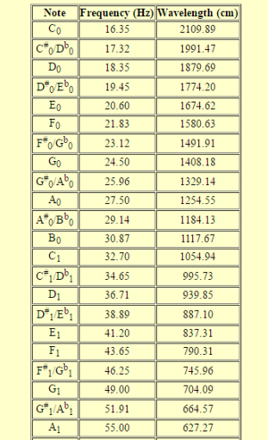
| + | * Initially, we had to figure out how a speaker worked and how to simulate a specific note on a speaker. As mentioned in the previous section, a speaker works by vibrating a membrane according to an analog voltage value. We figured that we needed to oscillate the speaker membrane at a specific frequency per note (as shown below). At that point, we needed to figure out which notes corresponded to which frequencies. After this, we had to figure out how to make the membrane move in a fashion is similar to a note's specific oscillation frequency. Realizing that this could be simulated by a sine wave, we wrote a similar function into the DAC to simulate each note. Several [http://www.phy.mtu.edu/~suits/notefreqs.html| notes and frequencies] are listed below. | ||
| − | [[File: | + | [[File:CmpE146 F16 T2 NoteFreq.PNG |thumb |center | <center> '''Figure 12. Sample of notes and frequencies in Hz. '''</center>]] |
| + | ===== Problems Encountered #2 ===== | ||
| + | *The precision of the frequencies was a significant limiting factor. If we were to use to RTOS default tick rate of 1ms (which in terms of frequency would be 1kHz), the number of audible notes we could simulate would have been very limited. Therefore, the tick rate had to be increased. We tried to implement a 100kHz tick rate, which would increase precision by a factor of 100. However, this seemed to crash the board. Therefore, it was decided that about 44kHz was a sufficient tick rate to simulate the frequencies we required. A discovery made during this experimentation was that the changing of tick rates also requires the disabling of the periodic scheduler task, which resets the microcontroller anytime the tick rate is not 1kHz. | ||
| + | === Full System Integration === | ||
| − | |||
| + | [[File:CmpE146 F16 T2 Glove.PNG |thumb | left | <center> '''Figure 13. Interfacing Flex Sensors with the Gloves '''</center>]] | ||
| − | |||
| − | * ''' | + | ===== Problems Encountered #1 ===== |
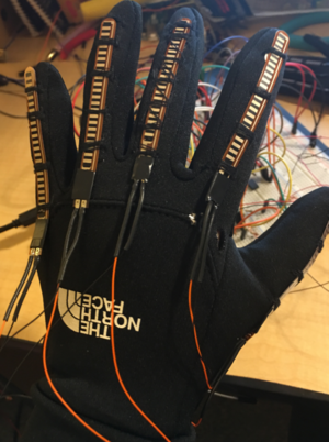
| + | * ''' Sewing: ''' Individually sewing the Flex Sensors onto the glove was very time consuming. In addition to that, it took a couple rounds to figure out which sewing method would be best for the sensor. In other words, the sensor had to be sewn tight enough to the glove so that it would not fall off, but loose enough to be able to flex freely. | ||
| + | * ''' Stabilizing the Base: ''' Another issue was to prevent the bottoms of the Flex Sensor from bending. As you can see in the Figure above, the ends of the Flex Sensors are covered with electrical tape. This aids in preventing unwanted damaged to the bottoms of the sensor. Once the base is overly bent the devices have a tendency to fail. | ||
| + | * ''' Soldering: ''' Lastly, we soldered wires to flex sensors so that it would be easier to interface with our other components. Due to the small gauge wire we used for the small ends of the sensors, the connections seemed to constantly break off. To fix this issue, shrink wrap was applied to keep the connections strong. | ||
| − | + | [[File:CmpE146 F16 T2 Speaker.PNG |thumb | right | <center> '''Figure 14. Audio Integration '''</center>]] | |
| − | |||
| − | |||
| − | |||
| − | ===== | + | ===== Problems Encountered #2 ===== |
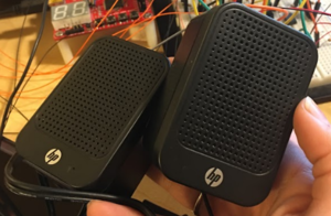
| − | + | * ''' Audio Integration: ''' Due to fault and different in part, we were experiencing differences with the way the audio sounded. Initially a Logitch speaker was purchased for the purpose of this project. However that speaker had internal rattling that was not fixable. Therefore, we switched to the speakers as seen in Figure 18.These were old and used speakers which actually started to die out on us during testing. | |
| − | + | * ''' Loose Connections: ''' Loose connections using jumper wires caused some sound quality issues. During testing we found that we would hear strange buzzes or rattles, initially we thought it was our algorithm and decided to further fine tune it. However, that was not the case, loose connections from the DAC to the breadbaord caused a decrease in sound quality. | |
| − | |||
| − | |||
| − | |||
| − | |||
| − | |||
| − | |||
| − | |||
| − | |||
| − | |||
| − | |||
| − | |||
| − | |||
| − | + | [[File:CmpE146 F16 T2 FullSystemPNG.PNG |thumb | left | <center> '''Figure 15. Full System Integration '''</center>]] | |
| − | ===== | + | ===== Problems Encountered #3 ===== |
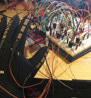
| + | * ''' Breadboard: ''' Since we choose to use a breadboard for faster prototyping purposes (as opposed to wire wrapping) we faced connectivity issues. The breadboard was defective in the fact that although our connections were solid, the interconnections inside of the breadboard were broken and therefore not actually connecting our circuit. We ended up buying another breadboard to solve this issue. | ||
| + | * ''' Exhaustive Testing ''' Individually the voltage divider circuits were set to specific values to trigger the when a specific voltage level was hit. After repeatedly using the gloves to test, the resistance on the sensors began to increase. This threw off our testing as the signals were not working as expected. Therefore during testing (depending on how much we used the sensor) we had to recalculate different resistances to make sure that the circuit still worked as expected. | ||
== Conclusion == | == Conclusion == | ||
| − | + | In conclusion, through this project, we were able to further our knowledge in Embedded Systems and FreeRTOS. We were able to successfully create our Piano Gloves. Through doing this we also learned a great deal about music, the importance of hysteresis, and algorithm development. If we were to do this project again, a better housing system for the Flex Sensors on the gloves would be implemented as they kept sliding out of their sewn positions. In addition to that, we would fine tune the algorithm a bit more to handle a more wide-variety of notes. As it is right now, our algorithm predominately handles lower notes better. Below you can find a list of the Hardware and Software Tradeoffs as well as a video demonstration of our project. Furthermore, a continuation of our project can also be found in the next section, were we added on a visualization aspect in response to a Piano Key Note being played. | |
=== Hardware & Software Tradeoffs === | === Hardware & Software Tradeoffs === | ||
| − | * DAC Precision (10-bit vs 12-bit) | + | * Onboard ADC vs Handmade ADC (handmade provided more flexibility) |
| − | * Sampling Frequency ( | + | * DAC Precision (10-bit vs 12-bit resolution, 12-bit provides 4X more res) |
| + | * Sampling Frequency (we found 44KHz was the optimal frequency to use) | ||
* Wave (Sine Approximation vs Square) | * Wave (Sine Approximation vs Square) | ||
** Sine offered smooth transition | ** Sine offered smooth transition | ||
| Line 534: | Line 576: | ||
=== Project Video === | === Project Video === | ||
| − | + | [https://youtu.be/c4x8iMNY2FQ Project Demo] | |
=== Project Source Code === | === Project Source Code === | ||
| − | * [https:// | + | * [https://github.com/ortizmelissa/PianoGloves Github Link] |
| + | |||
| + | == Optional == | ||
| + | |||
| + | === Visualization Development === | ||
| + | |||
| + | [[File:CmpE146 F16 T2 ParticleSystem.PNG | 1000px | center | <center> '''Figure 16. Piano Visualization '''</center>]] | ||
| + | |||
| + | === Software Used === | ||
| + | |||
| + | <center> Visualization Development Software Table </center> | ||
| + | |||
| + | <center> | ||
| + | {| class="wikitable" | ||
| + | |- | ||
| + | ! scope="col"| Item | ||
| + | ! scope="col"| Software | ||
| + | ! scope="col"| Type of Programming/Environment | ||
| + | |- | ||
| + | ! scope="row"|1 | ||
| + | | [https://unity3d.com/ Unity3D] | ||
| + | | Graphical Development | ||
| + | |- | ||
| + | ! scope="row"|2 | ||
| + | | Visual Basic | ||
| + | | C# | ||
| + | |} | ||
| + | |||
| + | </center> | ||
| + | |||
| + | === Visualization Design & Implementation === | ||
| + | |||
| + | In the above Figure is a Piano created in Unity3D by manipulating one its available assets. For the purpose of this project, a simple visualization was to be created to demonstrate the strike of a piano key. As you can see, there is a figure of a piano with some type of explosion. This is known as a particle system. The particle system was created to trigger once a finger was flexed from the Piano Gloves that we created. | ||
| + | |||
| + | * This part of the project is on-going and will most likely be continuing in development after duration of this class. This was an optional feature due to the fact that we wanted to focus on the Embedded Systems portion of this project rather than the Graphical design. | ||
== References == | == References == | ||
=== Acknowledgement === | === Acknowledgement === | ||
| − | + | We would like to thank the following people for expanding our knowledge in Embedded Systems: | |
| + | |||
| + | ''' Professors ''' | ||
| + | * [https://www.linkedin.com/in/preetpalkang Preet] | ||
| + | * [https://www.linkedin.com/in/haluk-ozemek-8708b23 Dr Ozemek] | ||
| + | |||
| + | ''' Lab Assistants''' | ||
| + | * [https://www.linkedin.com/in/praveenprabhakaran03 Praveen Prabhakaran] | ||
| + | * [https://www.linkedin.com/in/srinivasanshilpa Shilpa Srinivasan] | ||
=== References Used === | === References Used === | ||
| − | + | Listed below are references that were used in the development of this project: | |
| + | * [http://www.learningaboutelectronics.com/Articles/Flex-sensor-circuit-with-a-voltage-comparator.php Flex Sensor Basics] | ||
| + | * [https://youtu.be/Nrp8OgQLAlw Schmitt and Trigger Explanation] | ||
* [http://www.jstor.org/stable/pdf/3680062.pdf Digital Synthesis of Plucked-String and Drum Timbres] | * [http://www.jstor.org/stable/pdf/3680062.pdf Digital Synthesis of Plucked-String and Drum Timbres] | ||
| − | |||
* [http://citeseerx.ist.psu.edu/viewdoc/download?doi=10.1.1.8.8931&rep=rep1&type=pdf Commuted Piano Synthesis] | * [http://citeseerx.ist.psu.edu/viewdoc/download?doi=10.1.1.8.8931&rep=rep1&type=pdf Commuted Piano Synthesis] | ||
* [http://www.acoustics.ed.ac.uk/wp-content/uploads/AMT_MSc_FinalProjects/2012__Teng__AMT_MSc_FinalProject_PianoSynthesis.pdf Piano Sounds Synthesis] | * [http://www.acoustics.ed.ac.uk/wp-content/uploads/AMT_MSc_FinalProjects/2012__Teng__AMT_MSc_FinalProject_PianoSynthesis.pdf Piano Sounds Synthesis] | ||
| − | |||
| − | |||
* [http://users.ece.utexas.edu/~valvano/Volume1/E-Book/C13_DACSound.htm University of Texas on DAC and sound] | * [http://users.ece.utexas.edu/~valvano/Volume1/E-Book/C13_DACSound.htm University of Texas on DAC and sound] | ||
* [http://www.phy.mtu.edu/~suits/notefreqs.html Notes and Frequencies] | * [http://www.phy.mtu.edu/~suits/notefreqs.html Notes and Frequencies] | ||
| + | * [http://people.ece.cornell.edu/land/courses/ece4760/FinalProjects/f2015/swc63_ncm42_jmt329/swc63_ncm42_jmt329/webpage/index.html Piano Glove] | ||
| + | * [http://cmc.music.columbia.edu/musicandcomputers/chapter4/04_09.php Karplus Strong] | ||
| + | * [https://www.sfu.ca/sonic-studio/handbook/Sine_Wave.html Sine wave image from here] | ||
| + | * [http://www.nxp.com/documents/user_manual/UM10360.pdf LPC176x/5x User Manual] | ||
=== Appendix === | === Appendix === | ||
| − | + | Any references that we used can be found in the ''References'' section. | |
Latest revision as of 07:00, 24 December 2016
Contents
- 1 Project Title
- 2 Abstract
- 3 Objectives & Introduction
- 4 Schedule Overview
- 5 Parts List & Cost
- 6 Hardware Design & Interface
- 7 Software Design & Implementation
- 8 Conclusion
- 9 Optional
- 10 References
Project Title
OVS: Piano Gloves
Abstract
Music is in our everyday lives. Unfortunately, it is expensive to learn how to play an instrument. Therefore, we have decided to create Piano Gloves which can stand as a cheaper alternative to purchasing a Piano. This is a device that generates a fun piano-key note based on which finger is flexed. Our project gives the user flexibility in the types of notes that they would like to play. For instance, the user may select a Classic or 8-bit mode to access different note types. Please view our video at the bottom of the page for a live demonstration.
Objectives & Introduction
The objective of this project is to create a glove which can produce a specific piano-key note based which finger is flexed. To accomplish this task, we had to do the following:
- Purchase all necessary parts (as seen in the next section below)
- Simulate piano-key notes in MATLAB using the Karplus Strong Algorithm
- Port MATLAB Code to C using RTOS
- Sew Flex Sensors onto Gloves
- Create our own ADC circuit using OP-AMPS to handle 10 Analog inputs (1 per each finger)
- Configure the onboard DAC of the SJOne Board, as well as initializing GPIO ports
- Perform a full system integration for a finalized prototype
Optional Tasks
- Create a Real Time visualization based on which finger is flexed
Team Members & Responsibilities
- Full System Design
- Digital Signal Processing in MATLAB
- Device Driver Implementation
- Algorithm Development
- System Integration, Verification, and Validation Testing
- Visualization Development
- Algorithm Development
- Software Development
- Research on Music Frequencies and Design of Simulated Soundwaves
- Device Driver Implementation
- System Integration, Verification, and Validation Testing
Schedule Overview
| Week # | Start Date | End Date | Team Task Description | Status | Actual End Date |
|---|---|---|---|---|---|
| 1 | 10/14/16 | 10/21/16 | Research Design Approach and Assign Tasks | Complete | 10/21/16 |
| 2 | 10/21/16 | 10/28/16 | Set up Version Control and Research Parts | Complete | 10/28/16 |
| 3 | 10/28/16 | 11/4/16 | Discuss MCU Responsibilities and Communication | Complete | 11/4/16 |
| 4 | 11/4/16 | 11/11/16 | Purchase Parts and Begin Prototyping | Complete | 11/11/16 |
| 5 | 11/11/16 | 11/18/16 | Status Update: Demo First Round of Prototyping | Complete | 11/18/16 |
| 6 | 11/18/16 | 11/25/16 | Interface Modules and Perform System Design Verification/Validation Testing | Complete | 11/30/16 |
| 7 | 11/25/16 | 12/02/16 | Continue Validation and Optimize System | Complete | 12/05/16 |
| 8 | 12/02/16 | 12/20/16 | Finalize Design and Prepare for Demo | Complete | 12/18/16 |
Parts List & Cost
| Item # | Part Description | Vendor | QTY | Cost (USD) |
|---|---|---|---|---|
| 1 | SJOne Board | Preet | 1 | $80 |
| 2 | Flex Sensors | Mouser | 25 | $6.45 |
| 3 | MCP6242-E/P OPAMP | Mouser | 10 | $0.36 |
| 4 | 3.5mm Audio Jack | SparkFun | 1 | $0.95 |
| 5 | Gloves | Northface | 1 | N/A |
| 6 | Misc Parts (Wires, Resistors, Capacitors etc) | Personal | N/A | N/A |
- NOTE: Exact resistance values are not given for this project because they are different for each circuit. If you were to try to implement this project on your own, you would need to recalculate your individual resistances based on your respective Flex Sensors.
Software Used
- For this project, we implemented FreeRTOS which was provided to us by our instructor Preet. A download and tutorial of how to use it can be found here.
Hardware Design & Interface
Hardware Schedule
| Week # | Start Date | End Date | Description | Status | Actual End Date | Comments |
|---|---|---|---|---|---|---|
| 1 | 10/21/16 | 11/4/16 | Research Design Implementation and Brainstorm PCB Schematic Layout Determine and Purchase Parts |
Completed | 11/4/16 | |
| 2 | 11/4/16 | 11/11/16 | Design and Interface Schmitt Trigger Circutry w/SJOne Board Create PCB Schematic |
Completed | 11/11/16 | We determined that creating a PCB for this project was not necessary given the time constraints. |
| 3 | 11/11/16 | 11/18/16 | Sew Flex Sensors onto Gloves and Interface w/Development Board Status Update: Demo First Round of Prototyping |
Complete | 11/18/16 | Sewing the sensors onto the gloves was tedious. The sensors are very fragile, so they had to be handled with caution. |
| 4 | 11/18/16 | 11/25/16 | Integrate Hardware and Software, Perform System Design Verification/Validation Testing | Complete | 11/25/16 | |
| 5 | 11/25/16 | 12/02/16 | Continue Validation and Optimize System | Complete | 12/05/16 | |
| 6 | 12/02/16 | 12/20/16 | Finalize Design and Prepare for Demo | Complete | 12/18/16 |
Hardware Development
System Block Diagram
The following diagram is a high-level overview of our system. It is depicts the general structure of our design. In addition to that, it also demonstrates a generalization of the major system components that were used as well as their relationship among each other.
Flex Sensors
- How they work
A Flex Sensor is a passive device that can detect bending or moving. The resistance of the flex sensor changes whenever the metal pads (the side with the black stripe) are bent outward. As seen in Figure 1, the side with the thick black strips in the positive end and the side with the thin white strip is ground.
- How we used them
For this project, 10 Flex Sensors were used. Each Flex Sensor was individually hand-sewn onto a finger of the gloves. These sensors were used to detect finger movement by triggering a certain voltage threshold when a finger was flexed to a certain degree (more of this will be explain in the section below). A voltage divider was used to discover the variably changing resistance in the Flex Sensor. In other words, by forming a voltage dividing circuit, we were able to determine the resistance in response to a finger movement (Rflex) that was proportional to the voltage output. (If you are unfamiliar with voltage dividers, please find a quick tutorial along with the mathematical equations here.)
- NOTE: Since each flex sensors resistance is slightly different, an individual voltage divider circuit was prepared for each sensor.
- Flex Sensor Hook Up
As seen in Figure 2, a voltage dividing circuit was used to interface with the Flex Sensor. First, we must ground our device, so the ground end of the sensor was attached to ground. Next a resistor (Rn) was connected to VCC and the other end of it was connected to the positive end of the sensor. Afterwards, we placed an output wire in between the positive end of the sensor and the resistor to get the output voltage of the device. This was considered Vout (or our analog output) that was fed into our Schmitt and Trigger Circuit as mentioned below.
Schmitt and Trigger
- How it Works
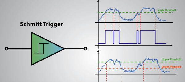
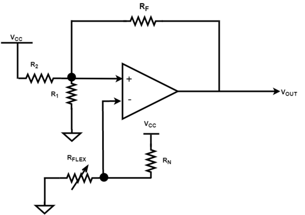
The Schmitt and Trigger circuit is a comparator with hysteresis. Hysteresis is the "dependence of the state of a system based on its history". In other words, it helps filter out signals so that the output reacts less reapidly than it normally would by using its previous output. It's a type of "memory" for the circuit. For this circuit in particular, it aids in preventing unwanted and frequent switching by cancelling out the noise. A demonstration of this can be seen in Figure 3. This is accomplished this by applying a positive feedback into the non-inverting terminal of the differential amplifier. By doing this, we are able to see if the circuit has "triggered" or hit a certain threshold (our threshold was between 1.1v and 2.2v). Below in Figure 4 is a schematic for the Schmitt and Trigger circuit that was used for this project.
- How we used it
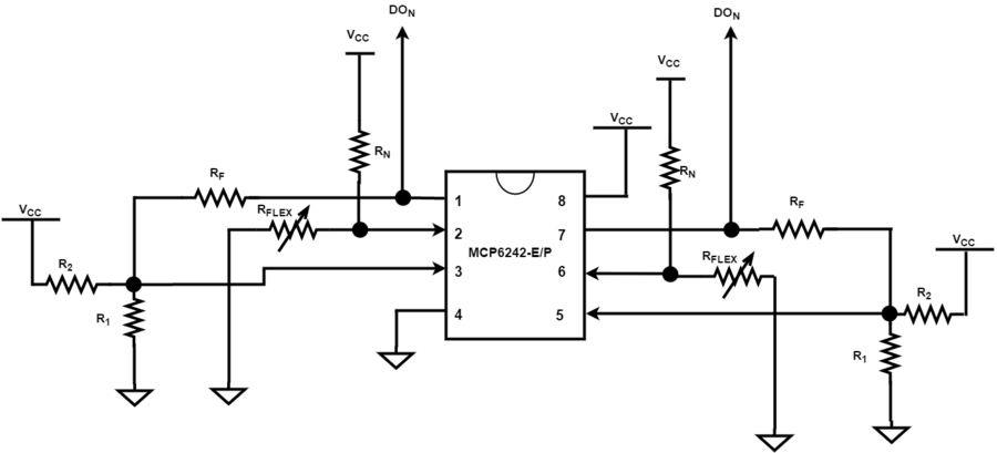
As seen in Figure 5, the Schmitt and Trigger Circuit was implemented with a MCP6242-E/P OP AMP. It was used to convert the Analog Output of the Flex Sensors into a Digital Signal. This Analog to Digital Conversion (ADC) was done so that the SJOne MCU could interpret the input signal using a GPIO port and then determine what to do with it. Since there were 10 signals that needed an ADC, Figure 5 was created a total of 5 times to account for producing 10 Digital Outputs (DO).
- Design Choice: We decided to create our own ADC circuit because of the limited availability on the SJOne board. There are simply not enough ADC pins to perform our task, as we would need 10 ADC pins.
SJOne Board
General Purpose Input/Output (GPIO)
As mentioned previously, GPIO pins from the SJOne Board were used to interpret the incoming signals produced from the Schmitt and Trigger. Below is a Pin Connectivity Table depicting the Pins we used, as well as their functionality.
GPIO: Pin Connectivity Table
| ITEM | PORT.PIN | DESCRIPTION | DIRECTION | CONNECTION |
|---|---|---|---|---|
| 1 | P0.0 | GPIO | INPUT | LEFT THUMB |
| 2 | P0.1 | GPIO | INPUT | LEFT INDEX |
| 3 | P0.29 | GPIO | INPUT | LEFT MIDDLE |
| 4 | P0.30 | GPIO | INPUT | LEFT RING |
| 5 | P1.19 | GPIO | INPUT | LEFT PINKY |
| 6 | P1.20 | GPIO | INPUT | RIGHT THUMB |
| 7 | P1.22 | GPIO | INPUT | RIGHT INDEX |
| 8 | P1.23 | GPIO | INPUT | RIGHT MIDDLE |
| 9 | P1.28 | GPIO | INPUT | RIGHT RING |
| 10 | P1.29 | GPIO | INPUT | RIGHT PINKY |
Digital to Analog Converter (DAC)
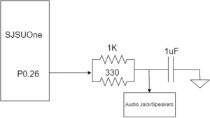
Below is a DAC connectivity table demonstrating the Pin Out of the DAC on the SJOne Board. Additionally, a block diagram has been provided to show how the DAC was interfaced with the Low Pass Circuit.
DAC: Pin Connectivity Table
| ITEM | PORT.PIN | DESCRIPTION | CONNECTION |
|---|---|---|---|
| 1 | P0.26 | DAC | LOW PASS FILTER |
- Design Choice Trade-Off: Due to time constraints and limited funding, we used the on-board 10-Bit DAC instead of purchasing a 12-Bit module. Since the on-board DAC is 10-Bits, we were only able to get 1K resolution, as opposed to 4K with a 12-Bit. Therefore the Analog Signal that was output to the Audio Speaker was not as precise as we hoped for.
Low Pass Filter
The Low Pass Filter was added to smooth out the signal that the DAC was providing. In other words, it enables signals with a lower frequency to pass through while attenuating signals that are above the cut off. By using this filter, we were able to get a better quality sound.
Datasheets
System Interface
Device Drivers
- GPIO: In order for the SJOne board to interpret the incoming signals from the Schmitt and Trigger Circuit, GPIO's had to be configured. Therefore we initialized 10 GPIO ports. First, we multiplexed the pins to select the proper configuration within their respective registers (LPC_PINCON->PINSEL0 or LPC_PINCON->PINSEL1) by using Bit Masking for GPIO Ports 0 and 1. Subsequently we configured each GPIO pin to be an input by using the FIODIR General Purpose Register (GPR). This allowed each pin to take in a voltage.
In order to determine whether a GPIO pin was receiving an input, a readGPIO function was implemented to read the current state of the digital port using the GPR FIOPIN.
- DAC: Similarly the DAC was configured as well. We had to use Bit Masking once more to properly multiplex P0.26 to be used as a Digital to Analog Output Pin. Next we configured the clock as well as began to write values into the DAC registers.
Software Design & Implementation
Software Schedule
| Week # | Start Date | End Date | Description | Status | Actual End Date |
|---|---|---|---|---|---|
| 1 | 10/21/16 | 10/28/16 | Research the following: Algorithm Design/Implementation and Digital Signal Processing in MATLAB |
Complete | 10/28/16 |
| 2 | 10/28/16 | 11/11/16 | Develop Karplus Strong Algorithm by incorporating RTOS, Create Device Drivers | Complete | 11/11/16 |
| 3 | 11/11/16 | 11/16/16 | Implement algorithm with DAC for simulation purposes | Complete | 11/16/16 |
| 4 | 11/11/16 | 11/18/16 | Status Update: Demo First Round of Prototyping | Complete | 11/25/16 |
| 5 | 11/18/16 | 11/25/16 | Implement Code w/Integrated Unit and Begin Debugging As Necessary | Complete | 12/02/16 |
| 6 | 11/25/16 | 12/02/16 | Continue System Integration Testing for Validation and Optimization | Complete | 12/07/16 |
| 7 | 12/02/16 | 12/20/16 | Finalize Design and Prepare for Demo | Complete | 12/18/16
|
Audio Algorithm Development
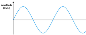
To discuss the audio algorithms, one must understand the notes that are being simulated. Audio frequencies correspond to certain notes. For example, a C4(commonly known as middle C on a piano) has a frequency of 261.63Hz. Sound waves are longitudinal and, simply put, create segments of compressed medium, such as air. A speaker converts an analog value to a sound by vibrating a membrane at a certain frequency, compressing and decompressing air(usually). Therefore, to simulate the note, we have to make the speaker play at that note's specific frequency. For that purpose, the DAC needs to send something similar to a sine wave function into the speaker to get sections of high and low compression.
This Project's Method to Simulating the Frequency
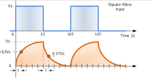
The initial plan of this project was to simulate a complete sine wave with 16 different values in a circular buffer. We would then use the vTaskDelay() function to simulate the space between the sine wave rise and fall increments. However, we found that with the possible tick rates, this led to too little precision in playback frequency. Beyond increasing the tick rate of RTOS, which we ran into issues with, we changed the design choice of using a sine wave. Due to the fact that the speaker needed sections of high and low voltage to create a sound, it was decided that we could send a square wave through the DAC and then use a hardware solution to create the curve of the sine wave, which was a low pass filter.
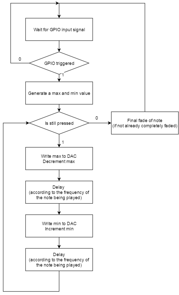
Algorithm Flowchart
Karplus Strong
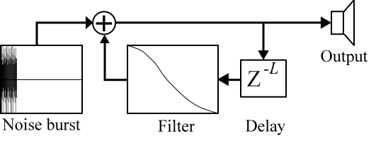
We also decided to use a Karplus strong algorithm, which simulates the fading of a note after is is played. Notes don't go on forever in real pianos, they fade. The algorithm decreases the amplitude by using a circular buffer, containing the wave, and averaging each element to a central value. Eventually, all the elements of the circular buffer would reach that central value and thus the amplitude (or difference between the highest and lowest value) would decrease. Therefore, to make the sound more real we used this algorithm.
Algorithm Diagram
Communication Protocols & Device Drivers
For our implementation, we are using GPIO ports and the onboard Digital-to-Analog Converter (DAC) of the SJOne Board. These are described below.
GPIO
The GPIO pins are configured to read the inputs of each finger of the gloves. If a finger is bent, the corresponding GPIO pin changes voltage levels. Upon reading this a key will be played.
Digital-to-Analog Converter (DAC)
The DAC we are using for this project is onboard the SJOne board. The DAC is used to communicate an analog signal with the speakers. The DAC we used has a resolution of 10 bits. It is modified by writing into DACR, which is the register for the DAC. By writing 10 single-bit values into this register, it converts the binary value to an analog value on the output pin of the DAC. This DAC has two sample frequency options, once every 1 microsecond or once every 2.5 microseconds. This is determined by a control bit in the DACR. For the purpose of precision, we decided to set this bit to 0, corresponding to a sample every microsecond.
Implementation
The steps required to initialize the GPIO pins were:
- Set the pin configuration to a GPIO
- Prepare the pin to be an input by setting it to a known value
The steps required to initialize the DAC were:
- Set the pin configuration to an Analog output
- Enable the clock for the DAC
- Write values into the DAC register
Hardware
Problems Encountered #1
- Wrong Parts: Initially we had ordered the wrong parts. Due to time constraints, we rushed selecting parts and were not careful on selecting the components that had the right packaging. Therefore, we ended up purchasing MSOPs (Mini-Small-Outlined-Package) instead of PDIPs (Plastic Dual Inlined Package). Using MSOPs would not work for us because the IC was simply too small to work with. It would not be able to fit on our breadboard for prototyping purposes. This caused a delay in our development; therefore, during this time, we focused on researching and developing the algorithm.
For more information on IC Packaging and Dimensions, please refer to this link: IC Package Dimensions
- Design Comment: Initially we were second guessing whether or not we needed a Schmitt and Trigger circuit for the purpose of this project. However, during testing we saw that it was easy to accidentally bend other fingers, or not hold a finger down for a certain duration of time. By implementing the Schmitt and Trigger Circuit, we were able to keep the signal high or low depending on if it was within the certain threshold (our threshold was between 1.1v and 2.2v). This enabled us to stop randomly firing other keys, and hold the ones we did want to play for the appropriate amount of time.
Software
DSP Simulations
In order to test the playing of notes through the DAC, we had to connect a speaker (or earphones) to the circuit so that we could hear the different sound frequencies that we were producing.
Problems Encountered #1
- Initially, we had to figure out how a speaker worked and how to simulate a specific note on a speaker. As mentioned in the previous section, a speaker works by vibrating a membrane according to an analog voltage value. We figured that we needed to oscillate the speaker membrane at a specific frequency per note (as shown below). At that point, we needed to figure out which notes corresponded to which frequencies. After this, we had to figure out how to make the membrane move in a fashion is similar to a note's specific oscillation frequency. Realizing that this could be simulated by a sine wave, we wrote a similar function into the DAC to simulate each note. Several notes and frequencies are listed below.
Problems Encountered #2
- The precision of the frequencies was a significant limiting factor. If we were to use to RTOS default tick rate of 1ms (which in terms of frequency would be 1kHz), the number of audible notes we could simulate would have been very limited. Therefore, the tick rate had to be increased. We tried to implement a 100kHz tick rate, which would increase precision by a factor of 100. However, this seemed to crash the board. Therefore, it was decided that about 44kHz was a sufficient tick rate to simulate the frequencies we required. A discovery made during this experimentation was that the changing of tick rates also requires the disabling of the periodic scheduler task, which resets the microcontroller anytime the tick rate is not 1kHz.
Full System Integration
Problems Encountered #1
- Sewing: Individually sewing the Flex Sensors onto the glove was very time consuming. In addition to that, it took a couple rounds to figure out which sewing method would be best for the sensor. In other words, the sensor had to be sewn tight enough to the glove so that it would not fall off, but loose enough to be able to flex freely.
- Stabilizing the Base: Another issue was to prevent the bottoms of the Flex Sensor from bending. As you can see in the Figure above, the ends of the Flex Sensors are covered with electrical tape. This aids in preventing unwanted damaged to the bottoms of the sensor. Once the base is overly bent the devices have a tendency to fail.
- Soldering: Lastly, we soldered wires to flex sensors so that it would be easier to interface with our other components. Due to the small gauge wire we used for the small ends of the sensors, the connections seemed to constantly break off. To fix this issue, shrink wrap was applied to keep the connections strong.
Problems Encountered #2
- Audio Integration: Due to fault and different in part, we were experiencing differences with the way the audio sounded. Initially a Logitch speaker was purchased for the purpose of this project. However that speaker had internal rattling that was not fixable. Therefore, we switched to the speakers as seen in Figure 18.These were old and used speakers which actually started to die out on us during testing.
- Loose Connections: Loose connections using jumper wires caused some sound quality issues. During testing we found that we would hear strange buzzes or rattles, initially we thought it was our algorithm and decided to further fine tune it. However, that was not the case, loose connections from the DAC to the breadbaord caused a decrease in sound quality.
Problems Encountered #3
- Breadboard: Since we choose to use a breadboard for faster prototyping purposes (as opposed to wire wrapping) we faced connectivity issues. The breadboard was defective in the fact that although our connections were solid, the interconnections inside of the breadboard were broken and therefore not actually connecting our circuit. We ended up buying another breadboard to solve this issue.
- Exhaustive Testing Individually the voltage divider circuits were set to specific values to trigger the when a specific voltage level was hit. After repeatedly using the gloves to test, the resistance on the sensors began to increase. This threw off our testing as the signals were not working as expected. Therefore during testing (depending on how much we used the sensor) we had to recalculate different resistances to make sure that the circuit still worked as expected.
Conclusion
In conclusion, through this project, we were able to further our knowledge in Embedded Systems and FreeRTOS. We were able to successfully create our Piano Gloves. Through doing this we also learned a great deal about music, the importance of hysteresis, and algorithm development. If we were to do this project again, a better housing system for the Flex Sensors on the gloves would be implemented as they kept sliding out of their sewn positions. In addition to that, we would fine tune the algorithm a bit more to handle a more wide-variety of notes. As it is right now, our algorithm predominately handles lower notes better. Below you can find a list of the Hardware and Software Tradeoffs as well as a video demonstration of our project. Furthermore, a continuation of our project can also be found in the next section, were we added on a visualization aspect in response to a Piano Key Note being played.
Hardware & Software Tradeoffs
- Onboard ADC vs Handmade ADC (handmade provided more flexibility)
- DAC Precision (10-bit vs 12-bit resolution, 12-bit provides 4X more res)
- Sampling Frequency (we found 44KHz was the optimal frequency to use)
- Wave (Sine Approximation vs Square)
- Sine offered smooth transition
- Square wave offered precision and allowed for filter to do the curving of the wave
Project Video
Project Source Code
Optional
Visualization Development
Software Used
| Item | Software | Type of Programming/Environment |
|---|---|---|
| 1 | Unity3D | Graphical Development |
| 2 | Visual Basic | C# |
Visualization Design & Implementation
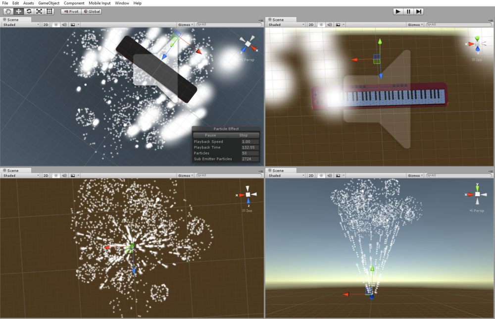
In the above Figure is a Piano created in Unity3D by manipulating one its available assets. For the purpose of this project, a simple visualization was to be created to demonstrate the strike of a piano key. As you can see, there is a figure of a piano with some type of explosion. This is known as a particle system. The particle system was created to trigger once a finger was flexed from the Piano Gloves that we created.
- This part of the project is on-going and will most likely be continuing in development after duration of this class. This was an optional feature due to the fact that we wanted to focus on the Embedded Systems portion of this project rather than the Graphical design.
References
Acknowledgement
We would like to thank the following people for expanding our knowledge in Embedded Systems:
Professors
Lab Assistants
References Used
Listed below are references that were used in the development of this project:
- Flex Sensor Basics
- Schmitt and Trigger Explanation
- Digital Synthesis of Plucked-String and Drum Timbres
- Commuted Piano Synthesis
- Piano Sounds Synthesis
- University of Texas on DAC and sound
- Notes and Frequencies
- Piano Glove
- Karplus Strong
- Sine wave image from here
- LPC176x/5x User Manual
Appendix
Any references that we used can be found in the References section.
